€1.00Original price was: €1.00.€0.00Current price is: €0.00.
Out of stock
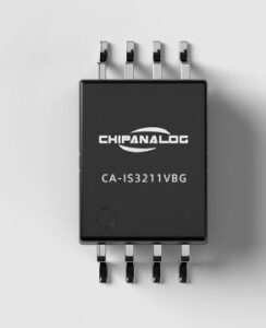
Isolated Single-Channel Gate Driver
Contact FMG for a quote or samples for evaluations
Each price quantity has minimum unit price. Prices reflect on how many units you purchase. Unit prices are divided up into 5 different price quantities. The more quantities you purchase the lower the price unit will cost you. Choose how many you want to purchase and when you add to cart your price will be calculated. To view your bulk price please go to the checkout or cart page.
The CA-IS3211 is an optocoupler-compatible single-channel isolated gate driver, designed for driving MOSFET, IGBT and SiC devices. The isolation level reaches 5.7kVRMS, and the chip can provide 5A sourcing and 6A injecting peak current capabilities.
The CA-IS3211’s supply voltage range up to 30V allows for the use of bipolar supplies, efficiently driving IGBTs and SiC power FETs. The chip’s performance highlights include high common-mode transient immunity (CMTI), low propagation delay, and low pulse width distortion. Strict process control ensures the chip’s consistency.
The input stage features an analog diode, which offers better long-term reliability and aging characteristics than conventional optocoupler-isolated gate driver LEDs. The high performance and reliability of the chip make it suitable for various applications, including industrial power supplies, photovoltaic inverters, vehicle chargers, DC motor control, and automotive air conditioning and heating systems.
The CA-IS3211 is capable of driving power tubes on both the high-voltage and low-voltage sides. It is fully compatible with traditional optocoupler gate drivers and significantly enhances driving performance.
CA-IS3211 Isolated Gate Driver Characteristics
5.7kVRMS single-channel isolated gate driver with optocoupler input
The input stage has a maximum reverse withstand voltage of 7V and supports interlocking
Wide body SOIC6-WB/SOIC8-WB package, air gap and creepage distance greater than 8.5mm
Operating junction temperature range TJ: -40°C to 150°C
We use cookies on our website to give you the most relevant experience by remembering your preferences and repeat visits. By clicking “Accept”, you consent to the use of ALL the cookies.
This website uses cookies to improve your experience while you navigate through the website. Out of these, the cookies that are categorized as necessary are stored on your browser as they are essential for the working of basic functionalities of the website. We also use third-party cookies that help us analyze and understand how you use this website. These cookies will be stored in your browser only with your consent. You also have the option to opt-out of these cookies. But opting out of some of these cookies may affect your browsing experience.
Necessary cookies are absolutely essential for the website to function properly. These cookies ensure basic functionalities and security features of the website, anonymously.
Cookie
Duration
Description
cookielawinfo-checbox-analytics
11 months
This cookie is set by GDPR Cookie Consent plugin. The cookie is used to store the user consent for the cookies in the category "Analytics".
cookielawinfo-checbox-functional
11 months
The cookie is set by GDPR cookie consent to record the user consent for the cookies in the category "Functional".
cookielawinfo-checbox-others
11 months
This cookie is set by GDPR Cookie Consent plugin. The cookie is used to store the user consent for the cookies in the category "Other.
cookielawinfo-checkbox-necessary
11 months
This cookie is set by GDPR Cookie Consent plugin. The cookies is used to store the user consent for the cookies in the category "Necessary".
cookielawinfo-checkbox-performance
11 months
This cookie is set by GDPR Cookie Consent plugin. The cookie is used to store the user consent for the cookies in the category "Performance".
viewed_cookie_policy
11 months
The cookie is set by the GDPR Cookie Consent plugin and is used to store whether or not user has consented to the use of cookies. It does not store any personal data.
Functional cookies help to perform certain functionalities like sharing the content of the website on social media platforms, collect feedbacks, and other third-party features.
Performance cookies are used to understand and analyze the key performance indexes of the website which helps in delivering a better user experience for the visitors.
Analytical cookies are used to understand how visitors interact with the website. These cookies help provide information on metrics the number of visitors, bounce rate, traffic source, etc.
Advertisement cookies are used to provide visitors with relevant ads and marketing campaigns. These cookies track visitors across websites and collect information to provide customized ads.